


How a PV Cell Converts Solar Power Into Electrical Power: Photovoltaics #2
An explainer on the building blocks of solar power—photovoltaic (PV) cells and PV modules

Introduction
Imagine three chefs tasked with recreating a complex dish in a cuisine they’ve never worked with before. The first chef experiments through trial and error, combining ingredients, hoping to stumble upon the right combination.
The second chef follows detailed photographs and recipes precisely—a perfectly valid approach that often produces satisfactory results for standard dishes served in predictable contexts. This chef can quickly learn to prepare these dishes for typical situations.
The third chef, however, studies the underlying principles of cuisine— the mallard reaction, expressing the flavors from each spice, the perfect sauce mouthfeel, and the techniques to layer each element to shine in their own right. While this approach requires more initial investment, its value becomes apparent when facing unique challenges: adapting a dish for dietary restrictions while maintaining its essential character, scaling it for hundreds of diners without losing quality, or creating cost-effective variations that preserve the crucial elements. Understanding the purpose of each component and the mechanism of how they change the dish’s texture and flavor allows for maintaining the dish’s integrity in the face of changing customer demands.
This parallels technology implementation strategies. Following established patterns and solutions, like our second chef, is often efficient and appropriate for standard use cases. This approach can deliver reliable results quickly when the requirements align with common scenarios. However, when organizations need to optimize performance, reduce costs, or adapt technology for specialized needs, a deeper understanding of fundamental principles, like our third chef, becomes invaluable.
Just as a chef with deep culinary knowledge can innovate while maintaining a dish’s integrity, technologists who understand their technology’s core principles can engineer more efficient, cost-effective solutions when standard implementations don’t meet their requirements. Investing in deeper understanding pays dividends when you must push beyond conventional usage patterns to create optimized, innovative solutions.
How do chefs preparing cuisine apply to solar power and photovoltaic technology? For me, photovoltaics is a cuisine that I prepare for customers with many dietary restrictions. I dove deep into the topic to understand the core mechanisms that power this technology so I can cut costs and maximize the performance of the system. Today, we are covering some of the physics and chemistry that empower the photovoltaic cell and module, the building blocks through which solar power is captured. If you are working on solar power or a competing energy source, I think you should stay. If you are interested in the mechanisms of converting light into usable energy, I think you should stay. If you are not interested in diving deep into the physics behind photovoltaic technologies, you should skip this one.
If you haven’t already, check out the first article in this series, which answers the question: Can solar energy power all of humanity?
How Does Solar Work
One of my favorite engineering principles is to keep it simple, stupid. Photovoltaic (PV) modules, or solar panels, do just that. Instead of deploying complicated power plants that convert chemical potential energy into heat and electrical energy, photovoltaics use laminated solid-state materials that produce power when light falls upon them. They scale very simply. They can generate higher voltages by stacking PV modules in series and more current by putting more stacks in parallel.
The best products appear simple but abstract away the complex nature of their function. Photovoltaics are no different.
The Photovoltaic Cell
There are dozens of types of PV cells. The differences can be material selection, construction methods, and the ability to capture light at different frequencies. The field is roughly divided into crystalline silicon (cSi), thin film, multi-junction cells, and a broader field of emerging PV technologies. That being said, the industry is dominated by crystalline silicon cells, accounting for 95% of global commercial installations. Cadmium telluride (CdTe) thin-film photovoltaic cells represent the second most significant technology, capturing 5% of the global market. Notably, CdTe has achieved greater penetration in the United States, comprising 15% of commercial installations and growing, driven solely by the success of the US-based First Solar.

Crystalline silicon (cSi) can be categorized into monocrystalline and polycrystalline cells. Monocrystalline silicon PV cells get cut from a large single quartz crystal. Each crystal slice gets cut down to the correct shape and size like a butcher slices a hunk of ham for deli meat. In contrast, smaller quartz crystals get crushed down and fused into one big ingot in a fashion not too distant from how we manufacture SPAM. These ingots get thinly sliced into the layers that make up the polycrystalline cells. Monocrystalline cells have slightly improved efficiency and lifespan at the downside of increased costs relative to their polycrystalline counterparts. Both are made by layering an N-doped silicon sheet onto a P-doped silicon sheet and then surrounding those layers in conductive current collectors and glass. Don’t worry if you don’t know what that means; we will dig into each of these details later in the post.
CdTe panels comprise cadmium sulfide (Cds) and cadmium-tellurium (CdTe) layers. Both cadmium and tellurium are by-products of mining zinc and copper, respectively. They are vaporized, deposited onto conductive glass sheets, wired up, and sealed to create the solar cell.
Respecting the reality that most PV cells sold today are cSi, I will focus my explanations on silicon-based constructions and may occasionally interject some details on CdTe PV cells. However, the mechanisms described throughout this article can apply generally to many types of photovoltaic cells.

What are n- and p-doping? Doping is a technique for adding impurities to a material that changes its properties. It is used heavily in semiconductors to make structures like FETs, diodes, and photovoltaic cells. To outline the importance of doping, we first have to step back and cover the basics of the atomic structure and the valence conduction band.
At the atomic level, electrons organize themselves into distinct energy bands when atoms interact with each other or encounter electromagnetic forces. Atoms are like onions or ogres, full of layers. The center of the onion is the atom’s nucleus, containing positively charged protons and neutral neutrons that together determine the atom’s mass. Surrounding this nucleus are successive electron bands arranged like concentric shells. The innermost band can hold a maximum of two electrons, and this first band is present in all atoms, though hydrogen and helium possess only this single band. The previous band must be filled for an atom to add a new electron band. As these bands extend outward from the nucleus, their electron-holding capacity increases, with middle bands accommodating eight or more electrons. The valence band is the outermost band, which may contain between one and eight electrons.
The valence band is the highest occupied energy level of the atom and contains the electrons that are most likely to be used for chemical bonding or electrical conductivity. While hydrogen and helium’s valence bands can accommodate two electrons, all other elements have valence bands with space for eight. Atoms naturally seek stability by achieving a full valence band, which they accomplish through one of three mechanisms: attracting additional electrons to fill empty spaces, forming bonds with neighboring atoms, or releasing their valence electrons entirely. The figure below denotes these complete and stable bands in green and the incomplete bands in red. Today’s discussion about the donation or acceptance of an electron or the filling of a hole will all be about the movement of electrons in and out of the valence band.

Above the valence band sits the conduction band. It is the lowest unoccupied band, and electrons move freely within it and contribute to electrical current. The conduction band becomes important when thinking about a group of atoms together, like the crystalline structure of silicon. In this crystal, the conduction band from each adjacent atom is linked, allowing the electron to move across the entire structure. For an electron to leave the valence band and jump to the conduction band, it must receive sufficient energy; after that, it is free to travel throughout the crystal. The term is band-gap energy and is synonymous with the escape velocity required for a rocket to leave Earth’s gravitational field, but applied to an electron trying to escape the electromagnetic field of its host atom.

When atoms lose an electron to conduction, they now have an empty space where an electron could be—a hole. One peculiarity in the world of electrical engineering is that we talk about holes as particles in a similar fashion to that of an electron. If you are unfamiliar with the concept of a hole, you can think of it as a gap in the road while driving during heavy traffic.
Let’s imagine you start with a gap in front of the car in front of you.
As soon as the vehicle in front of you rolls forward, that gap is now before you.
You now move forward, moving the gap behind you.
Then, the car behind you does the same, and the gap moves further back.
On and on and on.
The electron is the car, and the hole is the gap between vehicles. The gap technically only moves when the cars do. Regardless, it is easier to think about a hole as a particle because following one moving hole is more manageable than following the movement of the countless electrons that jump forward for that hole to pass by. So, we will consider both electrons and holes as fundamental charge carriers as we explore the photovoltaic cell.
N-doping makes the material more negative by adding impurities with more valence electrons and increasing the base material’s likelihood of receiving an extra electron. N-doping gives the silicon crystal a lower bandgap energy, requiring less energy to donate an electron from the valence band into the conduction band. Silicon has four valence electrons, so common dopants have five valence electrons. Phosphorous, arsenic, and antimony are the most common atoms used for N-doped silicon. These five valence electron neighbors more often donate their electrons to nearby Si atoms; when atoms have more electrons than the protons in their nucleus, they become negatively ionized. The greater the imbalance of electrons, the more electronegative it is.
P-doping is adding materials with fewer valence electrons. These materials steal an extra electron or two, so more silicon atoms have holes and are more positively charged as a byproduct. P-doping also gives the silicon crystal a lower bandgap energy, reducing the energy to accept an electron from the conduction band into the valence band. P-type dopants for silicon, such as boron, gallium, and iridium, have three valence electrons.
Instead of doping, CdTe PV cells are made of two distinct crystals. Their n-layer is cadmium sulfide, known for excess electrons that are easily excited to the conduction band. The p-layer is cadmium telluride (CdTe), which has many holes that can absorb these electrons.
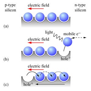
The real magic happens when the n- and p-doped layers join together. We will refer to the place where the layers meet as the junction. Remember that the n-doped material is electronegative, while the p-doped material is electropositive.
When the layers meet, the positively charged p-type material attracts the elections, which diffuse across the junction into the p-side. These electrons find plenty of holes to fill, recombining and entering the valence electron ring of the Si atom that hole was in. The n-doped material that loses electrons becomes more positively charged.
Meanwhile, the n-layer material attracts the holes from the p-side. They begin to diffuse to the n-side. As they move, these holes fill with the extra electrons in the n-layer. The p-doped material that fills its holes becomes more negatively charged.

The area immediately around the junction area loses its holes and electrons due to the attraction of the neighboring layer. We call that area, stripped of its charge carriers, the depletion zone. The increasing electronegativity of the p-layer and electropositivity of the n-layer at the junction area form a strong electric field across the depletion zone. This field begins to oppose the continued charge migration, preventing further electrons or holes deeper in the layer from approaching. Electrons on the n-layer don’t want to approach the negatively charged area of the p-layer in the depletion region. Like does not attract like. The same story occurs with the positively charged holes and the positively charged ions of the n-layer in the depletion zone. Current will stop flowing here until a larger external voltage is applied, which can once again force the charge carriers to pass through the depletion region and find new electrons and holes to combine with.
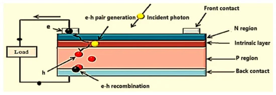
When a photon with an energy equal to the band-gap energy of the host material hits an atom in the PN junction, it excites a valence electron to the conduction band. The electron has met its escape criteria and can begin conducting. Luckily, visible light(400-700 nm) and infrared radiation(700-1000) have the energy to do this in Silicon and Cadmium Telluride.
The newly energized electron is drawn to the n-layer by positively charged silicon atoms in the n-layer’s depletion zone. At this same time, the hole where that first electron was trapped is filled by another electron from the p-layer, effectively moving the hole into the p-layer. Each time a photon of the right energy hits this junction, it forms another electron and hole pair. The current created by the flow of this electron and hole pair is called photocurrent and depends entirely on the amount of photons that hit the PV cell. The dependence on incident photons defines our first characteristic of the PV cell—short circuit current. We cannot make more current than the Sun provides photons. Even if we short both sides of the PV cell together, we would never get more electrons or current than light incident on the cell. We measure and discuss this amount of photons as electrical irradiance, a measure of watts per square meter.

One last note on the PN junction: It is a diode. Solar designers use several models to track cell performance; the most simplistic is the single-diode model. The model includes the following: a constant current source representing the photocurrent, a diode representing the PN junction, a series resistance representing the internal resistance of the cell, and a parallel resistance representing the leakage current past the cell.
The diode of the PN junction is opposite the direction of the power provided by the solar cells. The photocurrent will cause an electron to move to the n-layer and a hole to the p-layer. A diode in forward bias allows electrons to flow from the n-layer to the p-layer, with the opposite occurring in the hole direction. The diode of the PN junction does the same when the voltage applied to it is greater than or equal to the electric field generated by the depletion region. The current that flows through this diode (Id) does not flow through the load. Instead, this current allows the holes and electrons to recombine without doing any real work. When the PV cell’s generated current flows back through this diode, we reach our second characteristic of the PV cell—open circuit voltage (Voc). Given the solar irradiance and panel temperature, the PV cell’s open circuit voltage is the maximum voltage it can reach.

How can the voltage required to put the PN junction in forward bias be applied? The most common occurrence is caused by sunlight under the right conditions. The electrons and holes emitted by the photocurrent accumulate if they have nowhere to go. When there is an excess of electrons in the n-layer, it becomes more electronegative. The accumulated holes cause the p-layer to become more electropositive. These opposing charges create another electric field opposing the depletion region’s electric field. Charging up a voltage due to the charge accumulation works the same in the PV cell as in a capacitor.

Once the electric field of the accumulated charge is greater than the depletion region’s, the electrons and holes begin to recombine. The electrons head back to the p-layer, driving the holes doing the inverse. The point at which all electrons and holes have recombined is the open circuit voltage(Voc). The point at which the diode turns on when the PV cell electric field is equal to that of the depletion region is apparent when looking at the current versus voltage (IV) curve of a PV cell. It is the point at which the constant photocurrent begins to drop. The current through the PN diode increases exponentially with the voltage until all photocurrent passes through it. Like other diodes, this turn-on point changes significantly with the PV cell temperature.

As an engineer working on photovoltaic systems, I believe this built-in maximum voltage (Voc) is a considerable safety win. It prevents the voltage from continuing to charge to a hazardous degree, making it much safer than energy storage systems like batteries. When required, we can disconnect the PV array from a load and know the system won’t exceed this open circuit voltage level(Voc).
What do these PV cells look like? They are the small squares inside your solar panel. They may have small lines crisscrossing them and appear a deep blue or black.

Over the years, the PV cell has continued to grow in power, a byproduct of increased efficiency and size. It has taken on new features, like bifacial power absorption, generating light from both the top and bottom of the cell, and splitting cells when the PV cell is divided into two or more parts to reduce internal resistances.

The Photovoltaic Module (Solar Panel)
We know them as solar panels, but the broader renewable energy industry calls them photovoltaic modules, so begrudgingly, I will oblige. They are the smallest units in a PV array. They are the things we bolt down onto the sides of our roofs and plug together, like the adult version of LEGOs. With an installation that simple, it’s no wonder they have been the most installed form of energy in the US for the last 3 years running.1

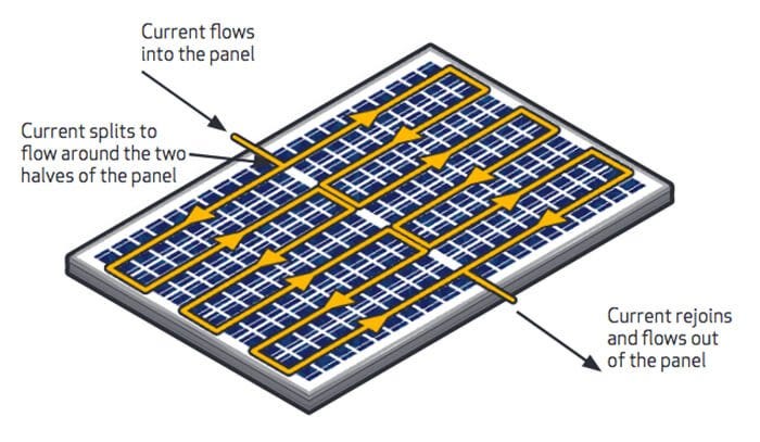
Your solar cells are stacked together, using custom busbars to connect each one electrically. They usually connect each cell in series.

They are stacked P->N->P, so when each cell creates its holes and electrons, the adjacent cell’s electrons consume holes, and vice versa for the electrons. Due to the fundamental nature of things in series, all the cells in the string have the same amount of current. So even if one cell gets less sunlight due to shading or damage, all the other cells in that string reduce their current output. The multiplication effect of one shaded cell affects all others in the same string, which is why partial shading significantly impacts the system’s performance.

Most modern solar panels build resiliency by splitting the solar cells in half and running the pieces in parallel strings. The parallel strings allow current to keep flowing on one side of the PV module, even if cells get shaded on the other half.
Modern solar panels also use bypass diodes to address the challenge of shaded cells. Typically, manufacturers install multiple diodes, with each diode short-circuiting an equal section of the cells in a string. Current can take this alternative path when one or more cells in that block see less light.
Here’s how it works: When shade covers one section of cells while others remain in full sunlight, they create less photocurrent than their unshaded counterparts, causing an electrical imbalance. The bypass diode only activates when the voltage at the panel’s negative terminal exceeds that of the healthy cell group. This activation occurs when the panel voltage drops to match the voltage produced by the unshaded cell groups.

This example shows a panel with a nominal voltage of 12 volts, three cell groups, and one unshaded group. Without activating the bypass diodes, the panel sees reduced currents corresponding to the degree to which the shaded cells are blocked from the incoming light. To activate the bypass diodes, the panel voltage decreases to one-third of the full system voltage, representing the proportion of unshaded groups to the total number of cell groups in the PV module. In this instance, the voltage of the unshaded group is around 4 volts, from which we will subtract the turn-on voltage of each of our bypass diodes, assumed to be around 0.3 volts. Since the PV cell is a current source and the PV cell voltage is based on the accumulation of charge carriers, the voltage only decreases by increasing the current demand of the load. As seen below in the violet, when the shading is significant, peak power can occur when the voltage is lower and the bypass diodes are active; power is voltage multiplied by current. Other times, when shading is not as significant, it may be a higher total power to maintain a higher voltage at a lower current.

Another source of variation in PV modules is whether or not they can accept light from two sides or just one side. Panels that only receive light from the top are monofacial, while those that absorb light from both sides are called bifacial.

Monofacial panels will have a glass top to allow light into the cell and a white plastic back sheet reflecting some light into the cell. They have an aluminum frame that holds the glass, bussing, PV cells, and backing sheet together. This frame adds rigidity since the back face is flimsy and a potential leak point in the PV module.
Bifacial panels have glass on both sides of the PV cell. The structural glass layers allow PV manufacturers to ditch the frame and its leak risks. It still keeps an aluminum edge seal that is useful for holding the edges together and as the attachment point to the panel’s mounting structure. On top of that, they have a higher rated power than their monofacial counterpart. Unsurprisingly, many commercial and utility-scale PV installations increasingly adopt bifacial panels due to their longer service life. This increase in adoption and supply has reduced their cost premium, versus monofacial panels, to a few cents or less per watt.

Bifacial PV modules capture light from both sides, harvesting direct sunlight and light that bounces off the ground onto their back surface.
The ground’s reflectivity, known as albedo, is crucial in this process. Think of albedo as nature’s mirror; some surfaces are excellent reflectors, like pristine snow or bright sand, while others, like dark shrubs and vegetation, barely reflect any light.
However, these panels have an interesting quirk in their design. The internal structure isn’t perfectly symmetric; the PN junctions are intentionally designed and manufactured with different layer thicknesses to maximize efficiency on the front face and minimize manufacturing costs. The asymmetry often reduces the back side’s ability to capture light. We measure this back-side performance as a percentage of the front face’s efficiency.
The mounting strategy becomes critical for bifacial panels to reach their full potential. Think of it like staging a play—you must ensure your audience (the panel’s back surface) has a clear view of the stage (the light). Mounting the panel too close to the ground or with any part of the back of the module blocked is like seating your audience behind a wall or a column; it reduces the ability of your audience to enjoy the play.
For this reason, residential roofs are not worth installing bifacial panels—the roof blocks most potential back-side generation. For home installations, stick with traditional monofacial panels. Save the bifacial technology for ground-mounted systems, where it can truly shine from both sides.

When mounting the PV module, both the bifacial and monofacial PV modules provide mounting points to hold the panel in place. These panels face forces from wind and snow, so they need to be relatively rigid. The most common method of holding the panel is clamping onto the aluminum edge seal, whether to a fixed frame or a rotating tracker system.

PV modules plugin simply, too. They come with connectorized flying leads, a term for wires coming out of the PV module. As far as I can tell, all solar panel manufacturers have standardized on the MC4 connector series, making the PV modules plug-and-play. They even come poke-yoked; the connectors are different on the positive and negative cables, making them less likely to be plugged in incorrectly. Pre-connectorization saves tons of time for installation and makes the skill level required to do so low enough for anyone to participate. Warning: these things get to high voltages, and proper training and personnel protective equipment (PPE) should always be used when working around high voltages.

What blew me away is the level to which PV modules are commoditized. If you look at the same year and similar power, they will all have the same open-circuit voltage, short-circuit current, diodes, variations due to temperature, and form factor down to 1-2% variance.
My background is working with battery systems. Batteries are commodities, too, but we will see significantly greater variations in internal resistance, voltage change over temperature, allowable charge, and discharge currents between each battery manufacturer. They are nowhere near as interchangeable as PV modules, meaning changes between suppliers are slow, costly, and have real technical risks.
It is starting to make sense to me why these things can get so cheap. There is no technical moat. Market share is determined by whomever has the best price. I would not want to be a PV module manufacturer; it seems cutthroat and brutal to turn a profit. But as someone who wants to use the power of the Sun to power our society more cheaply and cleanly, I am stoked about it.
U.S. Energy Information Administration. (2023, November 7). Solar photovoltaic module shipments hit a record high in 2022. https://www.eia.gov/todayinenergy/detail.php?id=61424